Coupled-Resonance Optical Waveguides
High hopes for the next generations of dense data transfer, ultrafast metrology, and biochemical sensing have energized the field of photonic chip design and set demands on fabrication processes. These exciting new devices leverage integration, power efficiency, enhanced light-matter interactions, and a large material range to make strides toward improving existing systems as well as envisioning a cadre of new light manipulation technologies from quantum com to medical diagnostics. An example of the device architectures receiving attention, and the focus of my work currently, is the photonic crystal coupled-resonator optical waveguide (CROW). In brief, by assembling a chain of cavities in close enough proximity to each other, a non-stationary state emerges which boasts the potential for dramatic optical slow-down, wavelength scale light confinement, and a split resonant structure all achievable on a chip the size of a pin-head.
Quantum Information Networks: Single Photon Transfer
Collaborative effort with Dr Michael Leuenberger and Hubert Seigneur. We take a dual-theoretical confirmation approach featuring their quantum mechanical model and my classical model in order to design
quantum information systems and move them toward
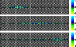
realization. The primary focus of the effort is the coupling of fixed computation centers (quantum dots in optical cavities) and a photonic network capable of routing and operating on single photons. In 2011 we reported 77% efficient energy density transfer of light from one cavity to another in a dynamically switched CROW system.
Fabrication: Photonic Crystal Slabs
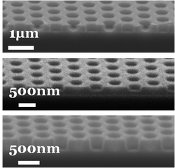
The fabrication of devices capable of achieving the goals outlined above is wrought with its own set of challenges. We focus on Silicon (passive) or Gallium-Arsenide (active) as material bases due to their high refractive index, and then employ electron-beam lithography to create the physical patterns that are on the order of a quarter of the wavelength of operation.
The structures shown here are the initial steps toward the fabrication of the devices discussed above. Imagery is made possible using Scanning Electron Microscopy (SEM) and all was done in-house at CREOL.
The structures shown here are the initial steps toward the fabrication of the devices discussed above. Imagery is made possible using Scanning Electron Microscopy (SEM) and all was done in-house at CREOL.
Publications:
Journal Publications
M.D. Weed, C.G. Williams, J.D. Ryckman, S.M. Weiss, P.J. Delfyett, W.V. Schoenfeld, Resonance uniformity of coupled-resonator optical waveguides, Optics Letters - submitted (April 2013)
M.D. Weed, C. Williams, P.J. Delfyett, W.V.Schoenfeld, Symmetry Considerations for Closed Loop Photonic Crystal Coupled Resonators, Journal of Lightwave Technology (2013)
H.P. Seigneur, M.D. Weed, M.N. Leuenberger, and W.V. Schoenfeld, Controlled On-Chip Single-Photon Transfer Using Photonic Crystal Coupled-Cavity Waveguides, (Invited Paper) Advances in OptoElectronics (2011)
Conference Proceedings
M.D. Weed, C. Williams, P.J. Delfyett, W.V.Schoenfeld, Feedback in coupled-resonance optical waveguides, CLEO 2012, Proc. OSA (2012)
M.D. Weed, H.P. Seigneur, and W.V. Schoenfeld, Cladding index engineering of the photonic properties of single-mode photonic crystal devices, Optics & Photonics 2010, Proc. SPIE, Vol. 7764, 776403 (2010)
M.D. Weed, H.P. Seigneur, M.N. Leuenberger, and W.V. Schoenfeld, Optimization of complete band gaps for photonic crystal slabs through use of symmetry breaking hole shapes, Photonics West 2009, Proc. SPIE, Vol 7223, pp. 72230Q-72230Q-9 (2009)
Presentations
H.P. Seigneur, M.D. Weed, G. Gonzales, and M.N. Leuenberger, and W.V. Schoenfeld, The Physics and Challenges of Realizing Quantum Teleportation Using Quantum Dots Within a Quantum Network, (Invited Talk) NanoFlorida (2009)
H.P. Seigneur, M.D. Weed, M.N. Leuenberger, and W.V. Schoenfeld, Self-assembled quantum dots within photonic crystal nanocavities for the realization quantum networks, (Invited Talk) Particles (2008)
